Introduction to PCB Controlled Impedance:
Connect two electrical devices (“driver” and “receiver”) for transferring signal power.
An increase in impedance will result if neighbours switch with the same polarity (Zoe, even mode). Conversely, a reduction in impedance will be sustained when the signal on a neighbouring trace switches with opposite polarity (Zoo, odd mode), resulting the potential effect of ghost signal and signal overlap and on overall product quality.
This needs extra attention when board traces carry high frequency. In this case, care must be taken to smooth a signal and to design traces matching the impedance of the driver and receiver.
The main factors affecting PCB Controlled Impedance are as follows:
* Dielectric thickness (52%);
* Dielectric constant (21%);
* Trace width/ space (18%);
* Copper thickness (6%);
* Solder (green) thickness (3%)…etc.
Calculating controlled impedance:
According to Polar’s multiple dielectric field solving controlled impedance design, there are three impedances: single ended impedance, differential impedance, and common mode impedance.
Depending on the calculations for inner and outer PCB layers, the selection of impedance (see diagram 1) and the controlled impedance calculations (see chart 1) may vary as described below.
To achieve accuracy of the actual controlled impedance, each PCB factory makes PCB boards with reasonable adjustments during the manufacturing processes. For example, when we edit CAM working files, we would add adjustments ensuring the good performance of etching and copper coating can be done. By doing so, we can prevent any potential effects on trace width/ space, as well as the differences from the actual product design, resulting manufacturing requirements cannot be met.
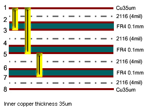
Diagram 1:
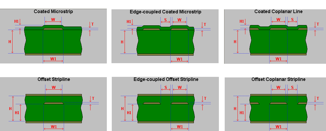
Chart 1:
|
Abb. |
Definition |
Characteristic Impedance |
Controlled Impedance Testing |
|
W / W1 |
Upper/ Lower Trace Width |
(Inverse): the smaller trace widths, the higher the series resistance. |
Per user prefs. |
|
S |
Separation |
(Direct): the larger trace space, the higher the series resistance. |
Per user prefs. |
|
T |
Trace Thickness |
(Inverse): the higher copper thickness, the lower the series resistance. |
Per actual product thickness. |
|
H |
Height |
(Direct): the higher dielectric thickness, the higher the series resistance. |
The general adjustment for controlling impedance; typically from 2.2mil~ 9.0mil. |
|
H1 |
Height 1 |
(Inverse): the higher solder thickness, the lower the series resistance. |
0.4mil ~ 0.6mil (In general). |
|
Er |
Dielectric Constant
(Characteristic of Thin-core material) |
(Inverse): the lower the dielectric constant, the higher the series resistance. |
Different dielectric materials lead to discrepancies between calculated and measured impedance values (i.e.: FR4 with dielectric constant ranges from 3.94 ~4.8). |
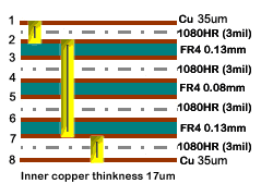
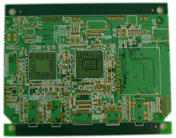
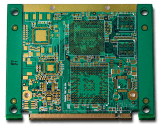
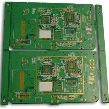
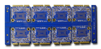
JetPCB’s recent productions associated to PCB controlled impedance testing:
|
Actual Product Photo |
Specification |
Stack-up |
 |
Layers: 10L
Thickness: 1.4 mm
Finished Copper : 1.0 oz
Board Size: 230mm*268mm
Surface Finish: Immersion Gold 3µ"
Min. Trace / Space: 3.5mil/ 3.5mil
Smallest Hole: 0.2mm
Special Specification:
Controlled Impedance: Total of 14
Single-ended 50ohm: 3.5, 4, 5mil
Differential 100ohm: 4/5, 4/12, 3.5/11mil
Single-ended coplanar 50ohm: 5/5/5mil
Differential coplanar 90ohm: 8/5/5/8mil
Differential coplanar 100ohm: 8/4/5/8mil |
 |
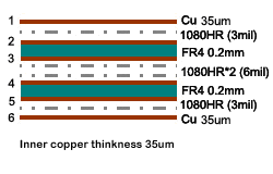
 |
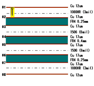
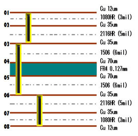
Layers: 8L
Thickness: 0.8mm
Finished Copper: 1.0oz
Board Size: 41 mm*57mm
Surface Finish: Immersion Gold 3µ"
Min. Trace / Space: 4mil/ 3mil
Smallest Hole: 0.1mm
Special Specification:
BGA 10mil/ Resin Plugged
Blind and buried vias: L1~L2, L8~L7, L2~L7
Controlled Impedance: Total of 3
Differential 70ohm: 8/7mil
Differential 100 ohm: 4/9mil |
 |
 |
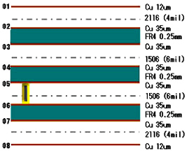
Layers: 6L
Thickness:1.0 mm
Finished Copper t:1.0oz
Board Size: 222mm*217mm
Surface Finish: Immersion Gold 3µ"
Min. Trace / Space: 3mil/ 5mil
Smallest Hole: 0.2mm
Special Specification:
Controlled Impedance: Total of 11
Single-ended 53ohm: 3.5mil
Single-ended coplanar 50ohm: 12/6/12mil
Differential 90ohm: 3.5/5.5mil
Differential 100ohm: 3/7.5mil |
 |
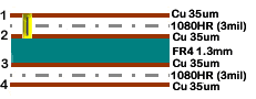
 |
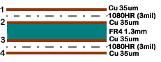
Layers: 4L
Thickness: 1.6 mm
Finished Copper: 1.0 oz
Board Size: 297 mm*208mm
Surface Finish: Immersion Gold 3µ"
Min. Trace / Space: 4mil/ 4mil
Smallest hole: 0.3mm
Special Specification:
Blind and buried vias:L1~L2
Controlled Impedance:
Differential100ohm :4.3/4mil,
|
 |
 |
Layers:4L
Thickness: 1.6mm
Finihed Copper: 1.0 oz
Board Size: 318mm*405mm
Surface Finish: HASL pb free
Min. Trace / Space: 4mil/ 4 mil
Smallest Hole: 0.2 mm
Special Specification:
Controlled Impedance: Total of 4
Single-ended 50ohm: 4.5mil
Differential 90ohm: 5.3/5mil
Differential100ohm: 4.3/5mil
|
 |
 |
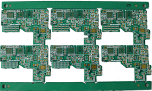
Layers: 8L
Thickness: 1.6mm
Finished Copper: 1.0oz
Board Size: 81mm*102mm
Surface Finish: Immersion Gold 3µ"
Min. Trace / Space: 4mil/ 4mil
Smallest Hole: 0.2mm
Special Specification:
BGA: 11.8mil
Blind and buried vias L1~L2
Controlled Impedance: Total of 6
Single-ended 50ohm:
Differential 90ohm:
Differential 100ohm |
 |
 |
Layers: 8L
Thickness: 1.2mm
Finished Copper: 1.0oz
Board Size: 70mm*90mm
Surface Finish: Immersion Gold 3µ" + Gold finger 3u”
Min. Trace / Space: 3mil/ 3mil
Smallest Hole: 0.2mm
Special Specification:
Blind and buried vias: L1~L3, L3~L6, L6~L8
Gold Fingers: 45 degree bevelling / Depth 20mil
BGA: 14mil / Resin Plugged
Controlled Impedance: Total of 20
Single-ended 40ohm: 6.5, 6.8mil
Single-ended 45ohm: 5.3, 5.5mil
Single-ended 48ohm: 4.8mil
Single-ended 50ohm: 4.3, 4.5mil
Single-ended 55ohm: 3.5mil
Differential 80ohm: 4.5/4.5mil
Differential 90ohm: 4.3/5.69mil
Differential 100ohm: 5.1/ 6.7mil |
 |
 |
Layers: 8L
Thickness: 1.6mm
Finished Copper: 1.0oz
Board Size: 145mm*147mm
Surface Finish: Immersion Gold 3µ"
Min. Trace / Space: 4mil/ 4mil
Smallest hole: 0.2mm
Special Specification:
Blind and buried vias L8~L7
BGA: 13mil
Resin Plugged
Controlled Impedance: Total of 6
Single-ended 50ohm: 6mil
Differential 90ohm: 6/8mil
Differential 100ohm: 7.5/8mil |
 |
 |
Layers: 8L
Thickness: 1.0mm
Finished Copper: 1.0oz
Board Size: 55mm*142mm
Surface Finish: Immersion Gold 3µ"
Min. Trace / Space: 4mil/ 4mil
Smallest Hole: 0.2mm
Special Specification:
BGA: 14mil
Gold Fingers
Blind and buried vias: L1~L3, L1~L5, L6~L7
Controlled Impedance: Total of 1
Differential 100ohm: 4/4mil |
 |
*Sources may refer to: TPCA Publication Rigid Circuit Board Materials Introduction.
The above are FYI, thank you.