Load board testing is mainly applied to check the functions and signals of the packed IC. Such test is given during the early manufacturing process to prevent the poor performance of the IC being made. It also reduces the chances of production costs spent on correction in the later process. Considering all of the above, such test is important for maintaining a company’s positive reputation.
Please find below some examples to the successful PCB prototypes that we have done:
|
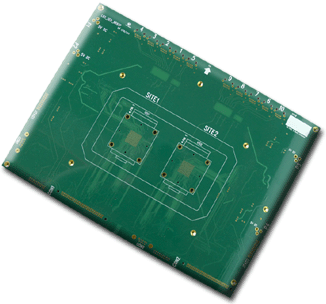
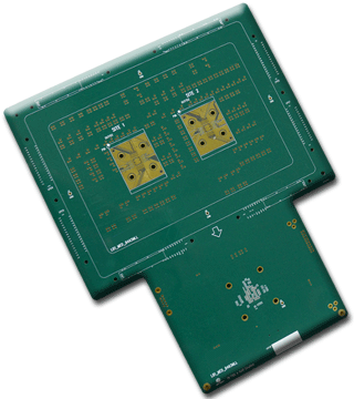
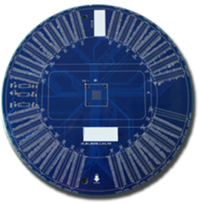
Actual Product Photo
|
Specification
|
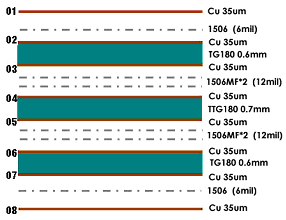
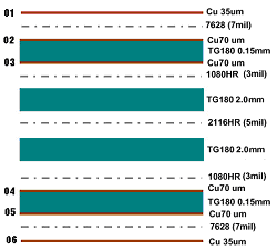
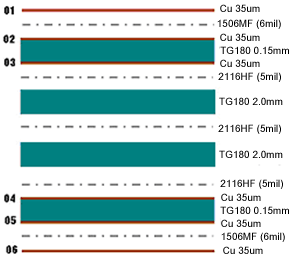
Stack-Up
|
|
|
Layers: 8L
Thickness: 3.0mm
Board Size: 325*395mm
Surface Finish: Immersion Gold 3u"
Min. Trace/Space : 4mil/ 5mil
Smallest Hole:0.2mm
Special Specification: Countersink
High Tg180 Material
Differential impedance 100ohm
|
|
|
|
Layers: 6L
Thickness: 5.0mm
Board Size: 280*347.5mm
Surface Finish: Immersion Gold 3u"
Min. Trace/Space: 5mil/5mil
Smallest Hole: 0.3mm
Special Specification:
High Tg180 Material
Differential impedance is 100ohm with a total of 2 batches |
|
|
|
Layers: 6L (Actual manufacturing layers: 10L)
Thickness: 5.1mm
Board Size: 336*336mm
Surface Finish: Immersion Gold 3u"
Min. Trace/Space: 4mil/2.2mil
Smallest Hole: 0.25mm
Special Specification:
High Tg180 Material |
|