Semiconductor Testing related to Printed Circuit Boards:
High frequency/ density characteristics for applications such as (vertical) probe card, load board…etc. resulted from the increasing specific requirements for impedance control, thickness, flatness and so on.
Please find below some examples to the successful PCB prototypes that we have done:
|
Actual Product Photo |
Specification |
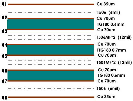
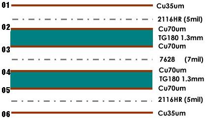
Stack-Up |
 |
Layers: 18L
Thickness : 5.0mm
Board Size: 292*429mm
Surface Finish: Immersion Gold 5u"
Min. Trace/Space:6mil/6mil
Smallest Hole: 0.3mm
Special Specification:
Countersinks
Impedance Control:
Single-ended 50ohm;
differential 90ohm; 100ohm with a total of 11 batches
|
|
|
|
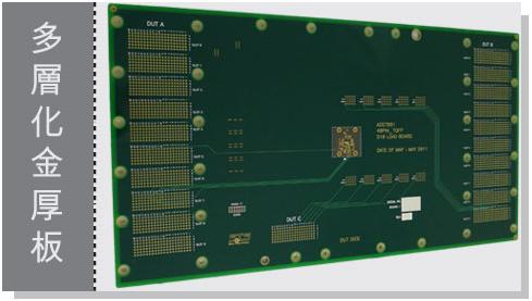
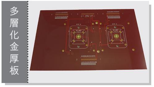
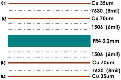
Layers: 6L
Thickness: 4.8mm
Board Size: 214*214mm
Surface Finish: Immersion Gold 3u"
Min. Trace / Space: 5mil/5mil
Smallest Hole: 0.25mm
Special Specification:
Countersinks
High Tg180 material
|
|
 |
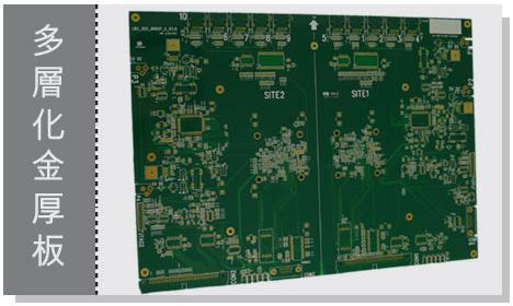
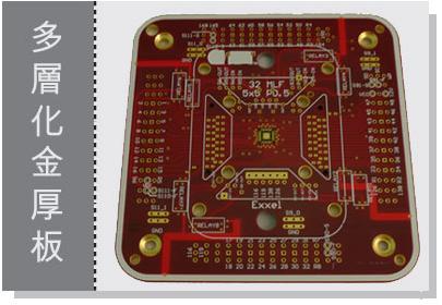
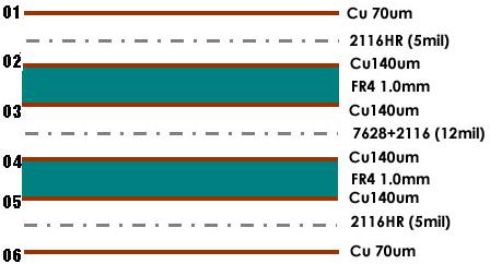
Layers: 6L
Finished Thickness: 5.0mm
Finished Size: 280*347.5mm
Surface Finish: Immersion Gold 3u"
Min. Trace Width/ Space: 5mil/5mil
Min. Diameter: 0.3mm
Special Specification:
High Tg180 material
BGA*29.5mil
Impedance control:
100ohm differential, a total of 2 batches
|
|
 |
Layers: 4L
Thickness: 3.3mm
Board Size: 121.9*121.9mm
Surface Finish : Immersion Gold 3u"
Min. Trace / Space: 8mil/8mil
Smallest Hole: 0.381mm
Special Specification:
High Tg180 material
Impedance control:
Single-ended 50ohm with a total of 2 batches
|
 |